- 您现在的位置:买卖IC网 > Sheet目录489 > NTLJD3181PZTBG (ON Semiconductor)MOSFET P-CH DUAL 20V 4A 6WDFN
�� �
�
�NTLJD3181PZ�
�Power� MOSFET�
�?� 20� V,� ?� 4.0� A,� m� Cool� t� Dual� P� ?� Channel,�
�ESD,� 2x2� mm� WDFN� Package�
�Features�
�?� WDFN� 2x2� mm� Package� with� Exposed� Drain� Pads� for� Excellent�
�Thermal� Conduction�
�?� Lowest� R� DS(on)� Solution� in� 2x2� mm� Package�
�?� Footprint� Same� as� SC� ?� 88� Package�
�?� Low� Profile� (<� 0.8� mm)� for� Easy� Fit� in� Thin� Environments�
�?� ESD� Protected�
�?� This� is� a� Pb� ?� Free� Device�
�V� (BR)DSS�
�?� 20� V�
�http://onsemi.com�
�R� DS(on)� MAX� I� D� MAX� (Note� 1)�
�100� m� W� @� ?� 4.5� V�
�144� m� W� @� ?� 2.5� V� ?� 4.0� A�
�200� m� W� @� ?� 1.8� V�
�Applications�
�?� Optimized� for� Battery� and� Load� Management� Applications� in�
�Portable� Equipment�
�?� Li� ?� Ion� Battery� Charging� and� Protection� Circuits�
�?� High� Side� Load� Switch�
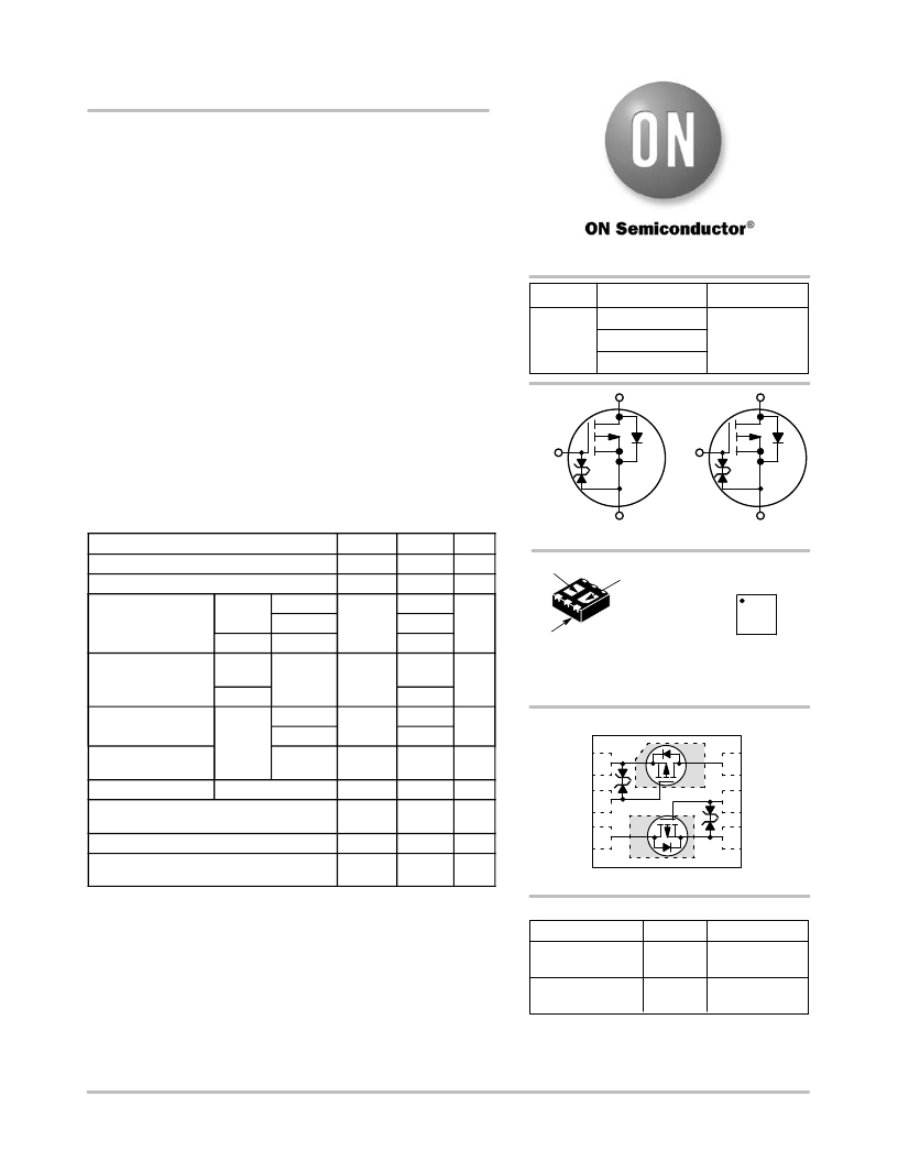
�G1�
�D1�
�G2�
�D2�
�MAXIMUM� RATINGS� (T� J� =� 25� °� C� unless� otherwise� noted)�
�Parameter� Symbol�
�Value�
�Unit�
�S1�
�P� ?� CHANNEL� MOSFET�
�S2�
�P� ?� CHANNEL� MOSFET�
�Drain� ?� to� ?� Source� Voltage�
�Gate� ?� to� ?� Source� Voltage�
�V� DSS�
�V� GS�
�?� 20�
�±� 8.0�
�V�
�V�
�D2�
�D1�
�MARKING�
�DIAGRAM�
�2� JEM� G�
�5�
�G�
�Continuous� Drain�
�Current� (Note� 1)�
�Power� Dissipation�
�(Note� 1)�
�Steady�
�State�
�t� ≤� 5s�
�Steady�
�State�
�t� ≤� 5s�
�T� A� =� 25� °� C�
�T� A� =� 85� °� C�
�T� A� =� 25� °� C�
�T� A� =� 25� °� C�
�I� D�
�P� D�
�?� 3.2�
�?� 2.3�
�?� 4.0�
�1.5�
�2.3�
�A�
�W�
�Pin� 1�
�WDFN6� 1� 6�
�CASE� 506AN�
�3� 4�
�JE� =� Specific� Device� Code�
�M� =� Date� Code�
�G� =� Pb� ?� Free� Package�
�(Note:� Microdot� may� be� in� either� location)�
�Continuous� Drain�
�Current� (Note� 2)�
�Power� Dissipation�
�(Note� 2)�
�Steady�
�State�
�T� A� =� 25� °� C�
�T� A� =� 85� °� C�
�T� A� =� 25� °� C�
�I� D�
�P� D�
�?� 2.2�
�?� 1.6�
�0.71�
�A�
�W�
�S1�
�1�
�PIN� CONNECTIONS�
�D1�
�6�
�D1�
�Pulsed� Drain� Current� t� p� =� 10� m� s�
�Operating� Junction� and� Storage� Temperature�
�Source� Current� (Body� Diode)� (Note� 2)�
�I� DM�
�T� J� ,� T� STG�
�I� S�
�?� 16�
�?� 55� to�
�150�
�?� 1.0�
�A�
�°� C�
�A�
�G1�
�D2�
�2�
�3�
�D2�
�5�
�4�
�G2�
�S2�
�Lead� Temperature� for� Soldering� Purposes� T� L� 260� °� C�
�(1/8� ″� from� case� for� 10� s)�
�Stresses� exceeding� Maximum� Ratings� may� damage� the� device.� Maximum�
�Ratings� are� stress� ratings� only.� Functional� operation� above� the� Recommended�
�Operating� Conditions� is� not� implied.� Extended� exposure� to� stresses� above� the�
�Recommended� Operating� Conditions� may� affect� device� reliability.�
�(Top� View)�
�ORDERING� INFORMATION�
�Device� Package� Shipping� ?�
�1.� Surface� Mounted� on� FR4� Board� using� 1� in� sq� pad� size� (Cu� area� =� 1.127� in� sq�
�[2� oz]� including� traces).�
�2.� Surface� Mounted� on� FR4� Board� using� the� minimum� recommended� pad� size�
�of� 30� mm� 2� ,� 2� oz� Cu.�
�NTLJD3181PZTAG�
�NTLJD3181PZTBG�
�WDFN6�
�(Pb� ?� Free)�
�WDFN6�
�(Pb� ?� Free)�
�3000/Tape� &� Reel�
�3000/Tape� &� Reel�
�?For� information� on� tape� and� reel� specifications,�
�including� part� orientation� and� tape� sizes,� please�
�refer� to� our� Tape� and� Reel� Packaging� Specification�
�Brochure,� BRD8011/D.�
�?� Semiconductor� Components� Industries,� LLC,� 2008�
�December,� 2008� ?� Rev.� 0�
�1�
�Publication� Order� Number:�
�NTLJD3181PZ/D�
�发布紧急采购,3分钟左右您将得到回复。
相关PDF资料
NTLJD3182FZTBG
MOSFET P-CH 20V 2.2A 6-WDFN
NTLJD3183CZTBG
MOSFET COMPL 20V LOW PRO 6WDFN
NTLJD4116NT1G
MOSFET N-CHAN DUAL 30V 6-WDFN
NTLJD4150PTBG
MOSFET P-CH DUAL 30V 3.2A 6WDFN
NTLJF3117PTAG
MOSFET P-CH 20V 2.3A 6-WDFN
NTLJF3118NTBG
MOSFET N-CH 20V 2.6A 6-WDFN
NTLJF4156NT1G
MOSFET N-CH 30V 2.5A 6-WDFN
NTLJS1102PTBG
MOSFET P-CH 8V 3.7A 6-WDFN
相关代理商/技术参数
NTLJD3182FZ
制造商:ONSEMI 制造商全称:ON Semiconductor 功能描述:Power MOSFET and Schottky Diode −20 V, −4.0 A, μCool? Single P−Channel & Schottky Barrier Diode, ESD
NTLJD3182FZTAG
功能描述:MOSFET 20V 4.1A UCOOL FETKY RoHS:否 制造商:STMicroelectronics 晶体管极性:N-Channel 汲极/源极击穿电压:650 V 闸/源击穿电压:25 V 漏极连续电流:130 A 电阻汲极/源极 RDS(导通):0.014 Ohms 配置:Single 最大工作温度: 安装风格:Through Hole 封装 / 箱体:Max247 封装:Tube
NTLJD3182FZTBG
功能描述:MOSFET 20V 4.1A UCOOL FETKY RoHS:否 制造商:STMicroelectronics 晶体管极性:N-Channel 汲极/源极击穿电压:650 V 闸/源击穿电压:25 V 漏极连续电流:130 A 电阻汲极/源极 RDS(导通):0.014 Ohms 配置:Single 最大工作温度: 安装风格:Through Hole 封装 / 箱体:Max247 封装:Tube
NTLJD3183CZ
制造商:ONSEMI 制造商全称:ON Semiconductor 功能描述:Power MOSFET 20 V/−20 V, 4.7 A/−4.0 A, μCool? Complementary, 2x2 mm, WDFN Package
NTLJD3183CZTAG
功能描述:MOSFET 20V 4.1A UCOOL CMPLM RoHS:否 制造商:STMicroelectronics 晶体管极性:N-Channel 汲极/源极击穿电压:650 V 闸/源击穿电压:25 V 漏极连续电流:130 A 电阻汲极/源极 RDS(导通):0.014 Ohms 配置:Single 最大工作温度: 安装风格:Through Hole 封装 / 箱体:Max247 封装:Tube
NTLJD3183CZTBG
功能描述:MOSFET 20V 4.1A UCOOL CMPLM RoHS:否 制造商:STMicroelectronics 晶体管极性:N-Channel 汲极/源极击穿电压:650 V 闸/源击穿电压:25 V 漏极连续电流:130 A 电阻汲极/源极 RDS(导通):0.014 Ohms 配置:Single 最大工作温度: 安装风格:Through Hole 封装 / 箱体:Max247 封装:Tube
NTLJD4114N
制造商:ONSEMI 制造商全称:ON Semiconductor 功能描述:High Efficiency DC-DC Converters
NTLJD4116N
制造商:ONSEMI 制造商全称:ON Semiconductor 功能描述:Power MOSFET